Note: This article is an English adaptation and technical revision of the original post published on SeanWangJS.github.io.
CUDA is a parallel computing platform and programming model built directly on top of NVIDIA’s GPU hardware architecture. Just as writing high-performance CPU software requires a solid grasp of CPU microarchitecture (caches, pipelines, SIMD extensions), writing efficient CUDA programs demands a foundational understanding of how GPUs are physically structured and how they execute workloads.
1. Starting from the Von Neumann Architecture
The classical Von Neumann architecture forms the bedrock of modern computing systems. It comprises five fundamental components: the Arithmetic Logic Unit (ALU), the Control Unit, Memory, Input devices, and Output devices. The ALU and Control Unit together constitute the Central Processing Unit (CPU). Memory encompasses primary storage (RAM) and secondary storage (disk/SSD), while input/output units form peripherals. Data moves between the CPU, memory, and peripherals across system buses.
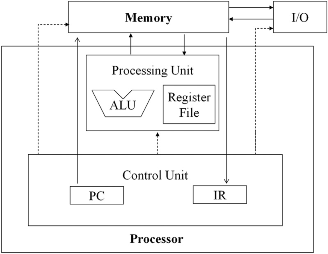 Figure 1.1: Classical Von Neumann CPU Architecture [1]
Over decades of rapid evolution, these basic units have grown immensely powerful and sophisticated. Modern CPUs operate at clock frequencies exceeding several gigahertz and house dozens of physical cores. Memory systems have evolved into deep, multi-tiered hierarchies comprising L1, L2, and L3 caches, main memory, and NVMe storage.
However, as Dennard scaling collapsed and Moore’s Law slowed down, scaling CPU performance solely by cranking up clock frequencies became thermally and physically prohibitive. Consequently, increasing the number of compute units and leaning into concurrency became the primary driver for performance growth.
This paradigm shift catalyzed the emergence of General-Purpose GPU computing (GPGPU). Structurally, GPUs extend the Von Neumann model by replicating the compute units (ALUs) at an unprecedented scale:
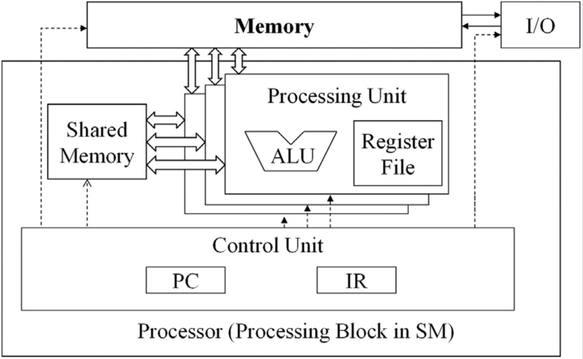 Figure 1.2: GPU-Enhanced Von Neumann Architecture [1]
Under this architecture, a single control unit orchestrates multiple execution/arithmetic units simultaneously. A single instruction is broadcast and executed across numerous execution units in parallel. This execution model is known as SIMT (Single Instruction, Multiple Threads), which is NVIDIA’s hardware-managed mechanism for implementing the broader SIMD (Single Instruction, Multiple Data) computing concept.
Key Distinction: CPU Multi-Core vs. GPU SIMT
The parallel design of GPUs operates on a fundamentally different plane than CPU multi-threading. A multi-core CPU features a small number of heavyweight, independent physical cores executing complex out-of-order execution pipelines. While CPUs also support SIMD (via vector instruction sets like SSE, AVX-512, and ARM Neon), they rely on wide vector registers (e.g., 256-bit or 512-bit registers) within a single thread context.
In contrast, a GPU devotes the vast majority of its silicon area directly to raw ALUs rather than large caches and branch predictors, allowing thousands of lightweight threads to run concurrently in hardware, organized and scheduled in lockstep units of 32 threads known as warps.
2. Streaming Multiprocessors (SM)
The Streaming Multiprocessor (SM) is the core computational building block of an NVIDIA GPU. Analogous to an independent CPU core (but massively wider), a modern GPU integrates dozens to over a hundred SMs.
Note on Physical Die vs. Commercial Product Configuration: The full GA100 physical silicon die (Ampere architecture) contains 128 SMs. However, to maximize manufacturing yield (harvesting partially defective dies), the commercial NVIDIA A100 GPU enables 108 SMs (or 56 SMs on A30). In the earlier Volta architecture, the GV100 physical die houses 84 SMs, with commercial V100 enabling 80 SMs.
Looking inside an individual SM, it is partitioned into four autonomous Processing Blocks (sub-cores). Each processing block operates as an independent SIMT execution unit:
- Control Hardware: Contains an Instruction Cache, a Warp Scheduler, and a Dispatch Unit.
- Compute Units: Houses an array of specialized execution units (CUDA Cores):
- FP32 Cores: Single-precision floating-point arithmetic.
- INT32 Cores: Integer arithmetic and memory address calculations.
- FP64 Cores: Double-precision floating-point arithmetic.
- Tensor Cores: Introduced in Volta and refined in Ampere/Hopper, Tensor Cores provide hardware-accelerated mixed-precision matrix multiply-accumulate () operations tailored for deep learning workloads.
In each A100 SM, there are 64 FP32 cores, 64 INT32 cores, 32 FP64 cores, and 4 third-generation Tensor Cores.
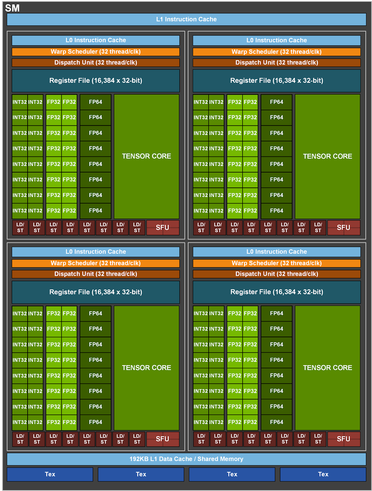 Figure 1.3: NVIDIA GA100 Streaming Multiprocessor (SM) Architecture [2]
3. GPU Memory Hierarchy
NVIDIA GPU memory architecture is structured into a multi-level hierarchy designed to hide DRAM access latencies through massive thread-level concurrency and high-speed on-chip SRAM:
- Registers: The fastest storage on the chip, private to each thread and allocated from a large physical register file (e.g., 256 KB per SM in A100).
- L1 Data Cache / Shared Memory: Ultra-fast on-chip SRAM located directly inside each SM. Starting with the Volta and Ampere architectures, L1 data cache and programmer-managed Shared Memory are unified into a single physical 192 KB SRAM pool per SM, dynamically configurable via CUDA runtime APIs (up to 164 KB dedicated to Shared Memory on A100).
- L2 Cache: A large on-chip cache shared across all SMs on the entire GPU (40 MB on A100, up to 50 MB on H100), providing high-bandwidth caching for global memory accesses.
- Device Memory (VRAM / Global Memory): Off-chip High Bandwidth Memory (HBM2/HBM2e/HBM3) or GDDR6 memory, offering large capacity (e.g., 40 GB / 80 GB) but higher access latency.
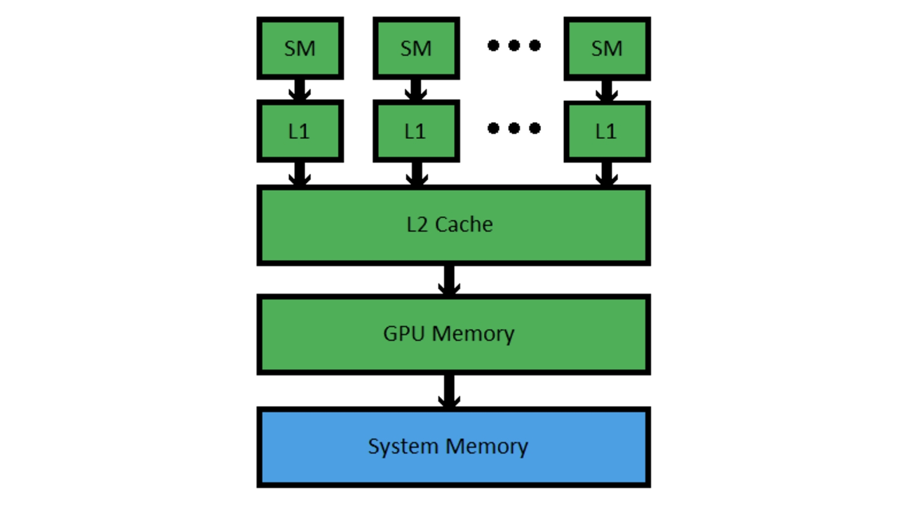 Figure 1.4: Simplified GPU Memory Hierarchy [3]
4. Memory Bandwidth
Memory Bandwidth measures the rate at which the Streaming Multiprocessors can transfer data to and from global device memory (VRAM), typically measured in GB/s or TB/s.
Because kernel execution involves memory latency and compute instruction dependencies, a real-world CUDA kernel rarely saturates 100% of theoretical peak bandwidth. Measuring and understanding theoretical bandwidth serves as a critical baseline for Roofline Modeling and evaluating whether a workload is memory-bound or compute-bound.
The theoretical peak memory bandwidth is computed as [4]:
- The factor of
2accounts for Double Data Rate (DDR) signaling, where data is transferred on both the rising and falling edges of each clock cycle.
Example: NVIDIA A100 (40 GB HBM2)
- Memory Bus Width: 5120 bits (5 active HBM2 stacks 1024-bit width per stack)
- Memory Base Clock Rate: 1215 MHz (effective data rate: )
This calculated throughput matches the official specifications published in NVIDIA’s hardware whitepaper [5].
5. Theoretical Peak Compute Performance (FLOPS)
GPU compute throughput measures the number of floating-point operations the processor can complete per second, expressed in FLOPS (Floating-point Operations Per Second), GFLOPS (), or TFLOPS ().
The theoretical peak throughput of standard CUDA Cores is defined as:
Why the factor of 2?
Modern GPU CUDA cores execute a Fused Multiply-Add (FMA) instruction in a single clock cycle: An FMA performs two arithmetic operations (one multiplication and one addition) in a single cycle, effectively doubling the floating-point operation throughput per core per cycle.
Example: NVIDIA A100 FP32 Peak Compute (Standard CUDA Cores)
- FP32 CUDA Cores per SM: 64
- Total Active SM Count (A100 SXM4): 108
- Boost Clock Rate: 1410 MHz ()
CUDA Core vs. Tensor Core Compute: The figure represents non-Tensor Core vector FP32 compute. When Tensor Cores are engaged (for matrix multiplications in deep learning), the A100 achieves in TensorFloat-32 (TF32) dense mode, and up to in FP16 dense mode, demonstrating the immense throughput advantage of dedicated matrix units.
6. Summary
Through this dual perspective of compute and memory, we arrive at two fundamental physical boundaries: peak memory bandwidth and peak compute throughput. Together, these two metrics establish the foundation of the Roofline Model, which helps determine whether a kernel is memory-bound or compute-bound.
In the next article, we will examine the CUDA programming model and see how software threads, blocks, and grids map onto these underlying hardware structures.
References
- D. B. Kirk and W. W. Hwu, Programming Massively Parallel Processors: A Hands-on Approach (PMPP), 4th ed., Section 4.4 on SIMD/SIMT Hardware.
- NVIDIA Corporation, NVIDIA Ampere Architecture In-Depth, NVIDIA Technical Blog.
- Supercomputing Blog, CUDA Memory and Cache Architecture.
- NVIDIA Corporation, How to Implement Performance Metrics in CUDA C/C++, NVIDIA Technical Blog.
- NVIDIA Corporation, NVIDIA A100 Tensor Core GPU Architecture Whitepaper.