Note: This article is an English translation and adaptation of the original post published on SeanWangJS.github.io.
CUDA stands for Compute Unified Device Architecture. It is a parallel computing platform and programming model built directly on top of NVIDIA’s GPU hardware architecture.
1. CUDA Compute Model
The CUDA compute model provides an abstraction over GPU execution units through a hierarchical computational structure. At its most granular level, the fundamental unit of execution is the thread. Logically, each thread is responsible for executing a portion of a larger computational task—such as adding a single pair of elements in a vector addition or computing a row-column dot product in matrix multiplication. By decomposing a macroscopic workload into thousands of lightweight threads, tasks can be scheduled at fine granularity to achieve massive parallelism.
Physically, a thread’s instructions are executed on a CUDA Core (historically termed a Stream Processor, or SP). In other words, each thread is mapped to an execution lane on a CUDA Core for processing, with the underlying hardware scheduling details abstracted away from the programmer by the CUDA runtime and hardware schedulers. One level above the thread is the thread block (or simply block), which consists of a group of threads and is assigned to a Streaming Multiprocessor (SM).
Here, we can observe a direct mapping between the physical hardware hierarchy (CUDA Cores and SMs) and the software abstractions (threads and blocks): each SM houses an array of CUDA Cores, just as each block comprises multiple threads. Because different GPU microarchitectures feature varying numbers of CUDA Cores per SM, programming directly against bare hardware would force developers to manually manage resource allocation across diverse device generations—a formidable challenge. Through CUDA’s abstraction layer, developers simply configure the thread layout, leaving hardware mapping and execution scheduling to the CUDA system, which substantially lowers the barrier to parallel programming.
Above the block level sits the grid, which encompasses multiple blocks. Together, these three tiers of abstraction—thread, block, and grid—allow developers to organize parallel workloads according to the geometric structure of their problem domain, enabling clean and scalable algorithm implementations.
Finally, between the thread and block levels lies an essential architectural concept: the warp. A warp consists of 32 threads and represents the fundamental unit of dispatch and execution in CUDA. All 32 threads within a warp are scheduled together and execute instructions in lockstep across execution units on an SM. This execution paradigm is known as SIMT (Single Instruction, Multiple Threads).
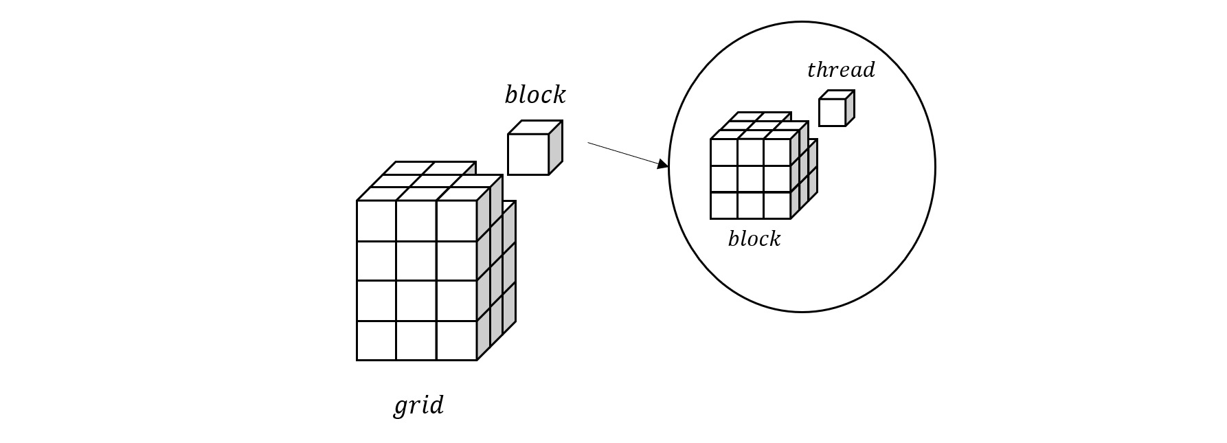 Figure 2.1: CUDA Compute Hierarchy [1]
Figure 2.1 illustrates the structural relationship among grids, blocks, and threads. Both grids and blocks can be configured with up to three dimensions (1D, 2D, or 3D), allowing individual blocks and threads to be indexed through coordinate tuples corresponding naturally to multidimensional data structures.
2. CUDA Memory Model
At the physical hardware level, GPU storage components consist primarily of register files, L1 caches, L2 caches, and off-chip device memory (VRAM). The CUDA programming model abstracts these physical structures into distinct logical memory spaces, each with its own scope, lifetime, and access performance characteristics:
- Registers
- Local Memory
- Shared Memory
- Global Memory
- Constant Memory
Among these spaces, registers and local memory are private to each individual thread; shared memory is shared across all threads within the same block; and global memory along with constant memory reside at device scope, remaining visible across all threads and persistent across multiple kernel launches.
Registers physically reside in the SM’s register file, delivering the highest read and write bandwidth with minimal latency. Shared memory is an on-chip memory space located within each SM. While shared memory operates as a logical address space, physically it resides on the same on-chip SRAM as the L1 cache. Consequently, shared memory and L1 cache are often discussed side by side; they share the same physical hardware resources, and their capacity partition can be dynamically configured through the CUDA runtime API.
Global memory, by contrast, maps to off-chip device memory (VRAM). Compared to on-chip storage, global memory incurs substantially higher access latency, though transfers can be accelerated and latency amortized through the hardware L1 and L2 cache hierarchies.
Local memory is used to store thread-private data that cannot fit into registers—such as thread-local arrays with dynamic indexing or variables spilled due to register exhaustion (register spills). Although physically backed by off-chip device memory, local memory accesses are cached in the L1 and L2 caches, mitigating access latency on cache hits while still incurring instruction and cache pollution overheads.
Similarly, constant memory (typically limited to 64 KB) is physically backed by device memory but cached in a dedicated on-chip constant cache. When all threads in a warp access the same memory location, the value is broadcast in a single cycle at near-register speeds; however, divergent accesses to different addresses are serialized.
3. CUDA Scheduling Model
Block Scheduling
The hardware entity corresponding to a thread block is the Streaming Multiprocessor (SM). An SM manages the execution of threads within the blocks assigned to it, provisioning required hardware resources such as registers and shared memory. Because the physical resources of an SM are finite, the number of blocks concurrently resident on an SM is strictly bounded by the aggregate resource footprint of those blocks. When all available SM slots become saturated, remaining blocks remain pending in a queue until earlier blocks complete execution and release their resources.
Warp Scheduling
Inside each SM, there are four autonomous processing blocks (sub-cores), each equipped with an independent Warp Scheduler. The warp scheduler is responsible for orchestrating the execution of warps assigned to its processing block. The entire set of warps resident on the block constitutes the pool of Active Warps. In each clock cycle, the scheduler examines these warps to determine which ones are ready to execute their next instruction without hazards (e.g., operands are ready and execution pipes are free); those ready warps form the set of Eligible Warps. The scheduler then selects an eligible warp and dispatches its instruction to the execution pipelines, designating it as the Issued Warp.
Thread Coordination and Execution
All threads belonging to the same block are guaranteed to be assigned to the same SM, enabling them to share a common on-chip shared memory space. Threads within a block can synchronize their execution using the barrier primitive __syncthreads(), ensuring that memory operations and shared states are consistent before proceeding with cooperative tasks.
The 32 threads within a warp execute instructions through the SIMT model: a single instruction is broadcast simultaneously across all active threads in the warp. When divergent execution paths arise—such as data-dependent conditional branches (if-else blocks)—the execution of divergent paths is serialized. Threads that do not participate in a given branch path are masked out (disabled) during that pass, a phenomenon known as warp divergence that reduces compute efficiency. In modern architectures (Volta and later), Independent Thread Scheduling (ITS) assigns each thread its own program counter and call stack, allowing finer-grained divergence and reconvergence, though programmers should use explicit primitives like __syncwarp() rather than assuming implicit lockstep execution.
References
- D. B. Kirk and W. W. Hwu, Programming Massively Parallel Processors: A Hands-on Approach (PMPP), 4th ed., Morgan Kaufmann, 2022.